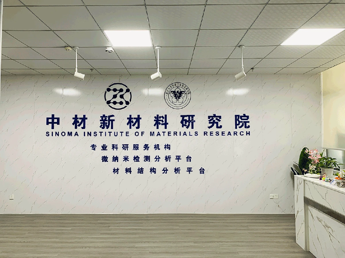
established in Guangzhou
Core services
One platform, complete analysis path
Organize testing around real research questions, not isolated instrument names.
01
Microstructure
SEM, TEM and morphology analysis for materials at micro and nano scale.
02Composition
Elemental, phase and distribution testing with traceable reports.
03Failure analysis
Find crack, defect and process causes through evidence chains.
04Performance testing
Connect structure, process and application behavior.
05Data analysis
Transform complex testing data into readable decisions.
06Technical consulting
Testing plans and technical support for R&D problems.
Solutions
Clear paths for complex materials
Biomaterials
Micro-nano characterization for biological and medical materials.
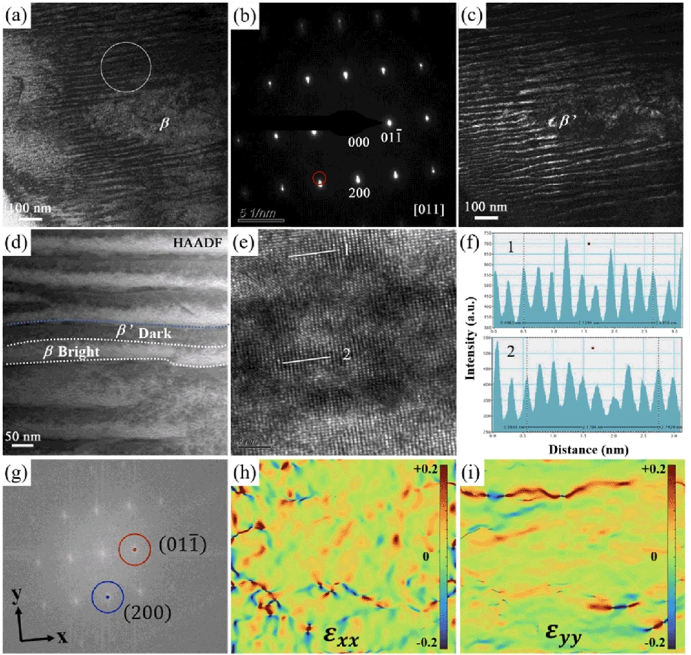
Metal materials
Grain, phase, inclusion and defect analysis for metal systems.
Inorganic non-metallic materials
Testing workflows for ceramics, glass and inorganic materials.
Polymer materials
Structure, morphology and composition analysis for polymer systems.
Two-dimensional materials
Morphology, phase and microstructure analysis for 2D materials.
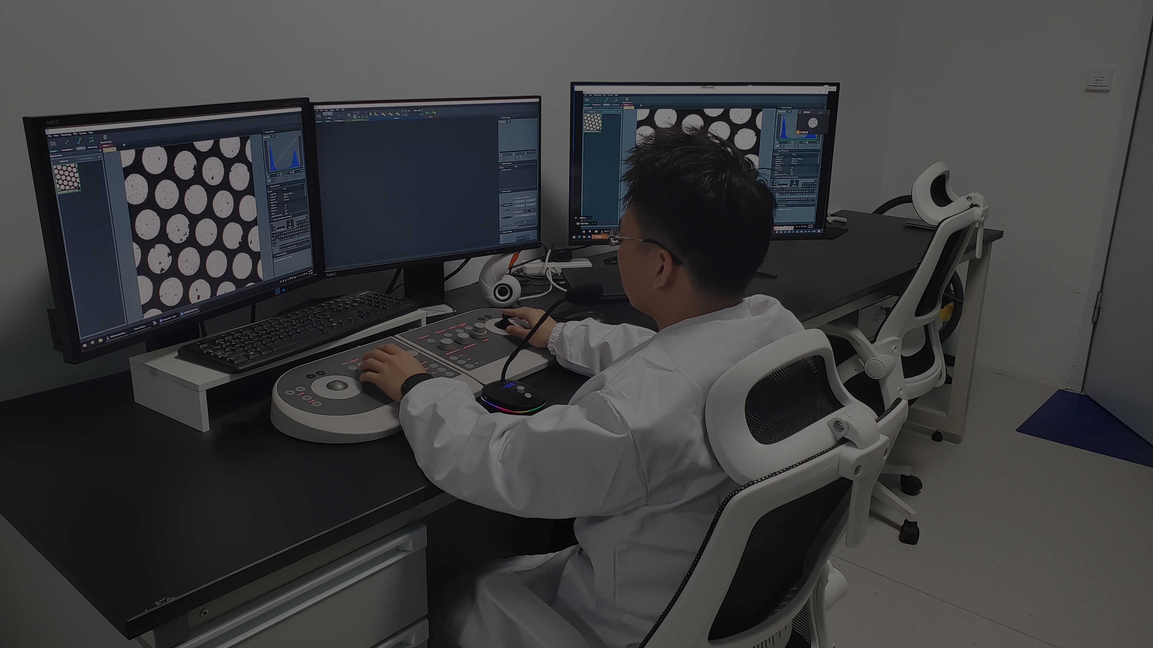
New materials R&D
Systematic testing support for research samples and papers.
Lab & equipment
See deeper with professional instruments
Instrument capability, analyst experience and report standards work together to make results reliable.
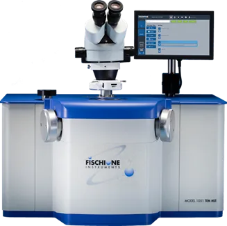
Ion thinning instrument
TEM sample preparation for multiple material systems.
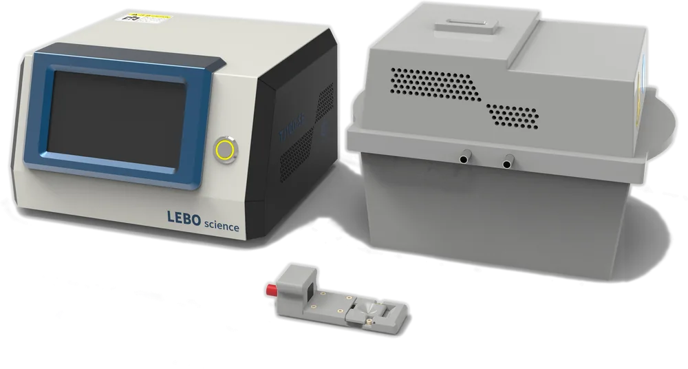
Twin-jet electropolisher
Electrolytic thinning for metal TEM samples.
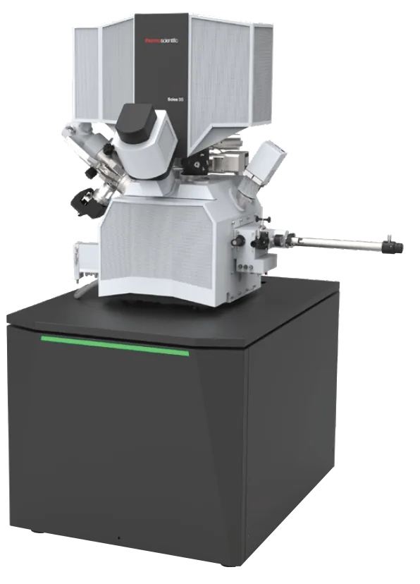
Focused ion beam equipment (FIB)
Site-specific cutting, thinning and micro-nano processing.
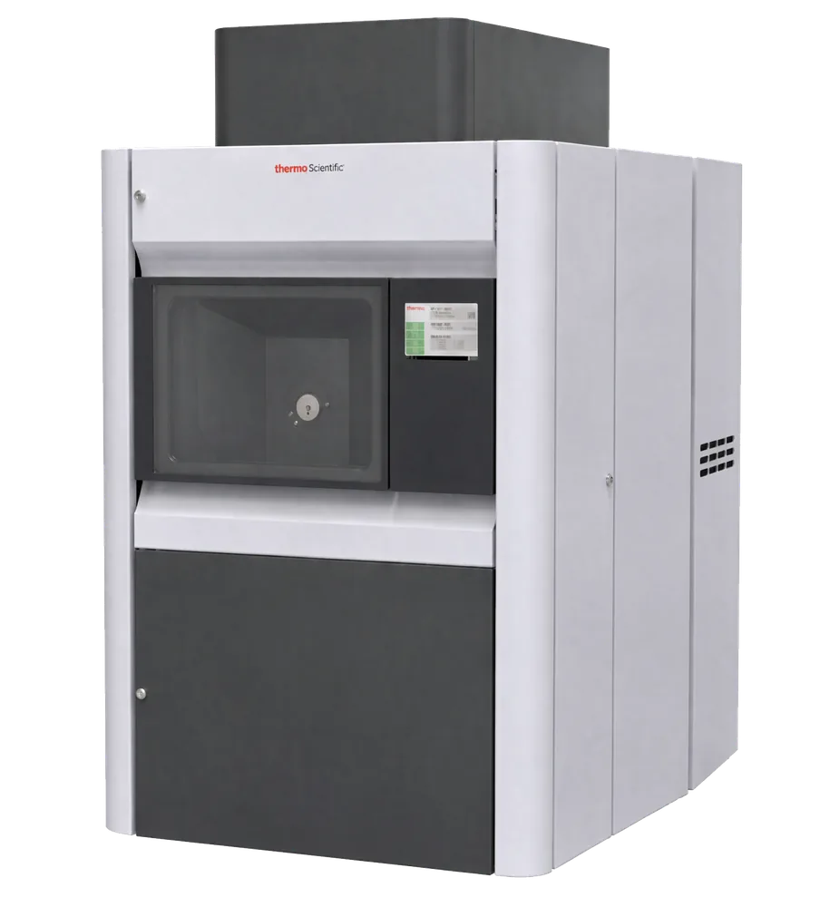
Talos F200X TEM
High-resolution transmission electron microscopy and composition analysis.
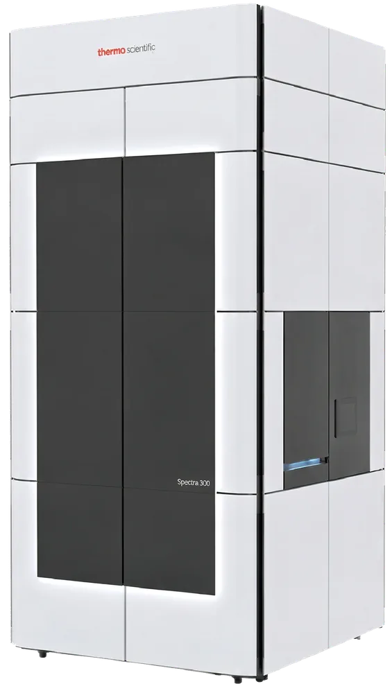
Spectra 300 aberration-corrected microscope
Atomic-scale imaging and fine structure characterization.
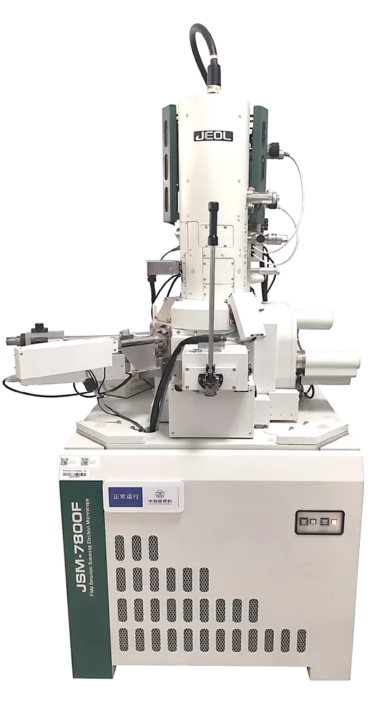
Field emission SEM
High-resolution surface and microstructure observation.
Testing process
From question to report
- 01Requirement
- 02Plan
- 03Sample receipt
- 04Testing
- 05Review
- 06Report
Strength
Reliable partners for trusted analysis
published service detail pages
published capability groups
equipment currently listed
analysis goals and material systems
company, industry and technical entries
Featured cases
Evidence chains matter more than one image
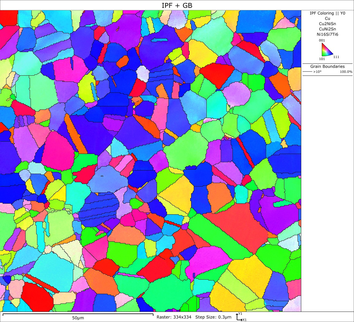
Metal material microstructure analysis
SEM/EBSD analysis for grain orientation and organization features.
Inorganic non-metal material characterization
XRD, SEM and TEM support structure and morphology analysis.
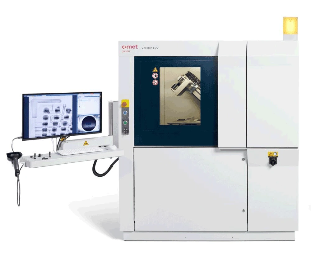
Semiconductor device failure analysis
X-ray, SAM and FIB help locate internal cracks and defects.
Coating microstructure analysis
SEM, TEM and EDS support coating morphology and composition evaluation.
Ceramic morphology and structure analysis
SEM/TEM characterization for ceramic and oxide material samples.
News
View more ›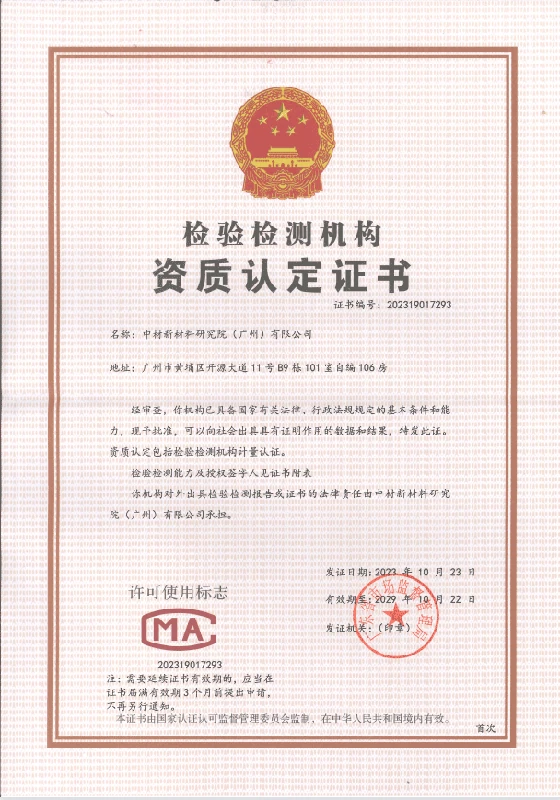 MicroEagle Analysis Center passed CMA accreditation and received its certificateThe center passed its initial CMA on-site assessment, marking a new stage in quality management and testing capability.
 MicroEagle Analysis was invited to the 2018 Youth Science and Technology ForumMicroEagle Analysis attended the forum and presented on microscopic testing methods for micro- and nano-devices.MicroEagle was invited to introduce electron microscopy to studentsA science-outreach session introduced materials analysis, transmission electron microscopy and nanostructure characterization to students.
 MicroEagle Institute selected as a 2022 Guangzhou “Seed Unicorn” enterpriseSinomat Institute ofMaterials Research (SIMR) was selected for Guangzhou’s 2022 Seed Unicorn enterprise list.MicroEagle Analysis Center passed CMA accreditation and received its certificateThe center passed its initial CMA on-site assessment, marking a new stage in quality management and testing capability.
FAQ
How do I choose a test?
Send the material type, sample condition and testing goal. We will help match a suitable workflow.
Does the sample need preparation in advance?
It depends on the testing method. SEM, TEM, EBSD, FIB and section analysis may require different preparation steps.
What if the SEM sample is not conductive?
Non-conductive samples may need gold or carbon coating to reduce charging effects before SEM observation.
What are the sample requirements for EBSD?
The testing surface should be smooth and flat, with minimal residual deformation. Ion polishing or electrolytic polishing may be used.
When is FIB sample preparation suitable?
FIB supports site-specific cutting and thinning, especially for cross-section or targeted TEM sample preparation.
What can metallographic sectioning observe?
It is commonly used to inspect cross-section structure, cracks, delamination, dimensions and local failure positions.
What does the testing report include?
The report usually includes testing conditions, images or data, analysis notes and conclusion suggestions.
Partners
Trusted by universities, institutes and advanced manufacturing partners








Professional materials analysis for your next decision
Send us your sample information and testing goal. We will help confirm the next step.
Contact us